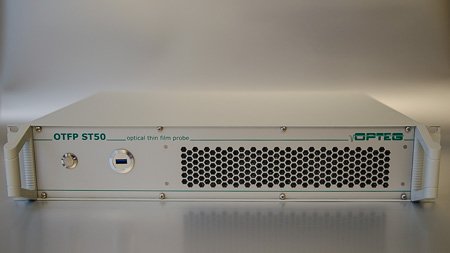
Optical film thickness (thin film) measuring device
The reflectometric thin film measurement is based on the principles of thin film interference. This makes it possible to determine the thickness of dielectric thin films and calculate the material’s refraction index from the data. Thin films are becoming increasingly widespread, and are used in the solar industry, for anti-reflection coatings or for coatings on medical implants.
The devices can be used to measure semi-transparent films and all kinds of semiconductor (both transparent and non-transparent). It is important that the film to be measured has at least one slightly glossy surface.
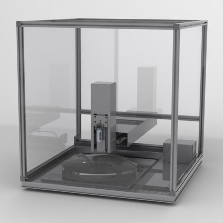
 We provide optical film thickness measuring devices for wavelengths of 180 to 2,500 nm that are suitable for a range of applications. Thanks to a sophisticated axis system, the OPTEG measuring devices can also be used for measuring large areas. The thin film measuring device features an integrated PC. It can act as a server and can be contacted using one or more software clients via a simple TCP/IP connection. This makes it possible to display the results simultaneously or use them at various points, such as for process control.
Have any questions? Get in touch! Find your contact partner here.
Where are extremely thin films used in industry?
Thin films are used as diffusion barriers or as insulators between conductive films, for example. They are also widely used as a hard coating against scratches (e.g. discs and plastics in the automotive industry) or as an anti-reflex coating (e.g. optical glasses, glass lenses). Thin film applications cover a size spectrum that ranges from less than 10 Å (equivalent to a few atoms) to 100 μm (comparable to the width of a human hair). These films are applied using processes such as spin coating, vacuum evaporation, sputtering, vapor deposition or dip coating. They must also be of exactly the right thickness to perfectly fulfill their purpose. Composition, roughness and other factors can also be decisive for the desired function.
Selection of measurable films
Silicon, SiO2, SiNx, DLC, polymer films, polyimides, polysilicon, amorphous silicon
Typical applications
Production of semiconductors: photoresist, oxides, nitrides
Liquid crystal displays: cell spacing, polyimides, ITO
Optical coatings: hardening coatings, anti-reflective coatings, filters
Technical data
| Measuring range (depending on film arrangement) 50 | 50 nm - 50 μm |
| Spectrometer wavelength range | 200 - 1100 nm |
| Spectrometer resolution | 2048 Pixel |
| Precision (without axis system, depending on film arrangement) | +/- 1 nm |
| Reproducibility (without axis system, depending +/- 0,1 nm on fi lm arrangement) | +/- 0,1 nm |
| Electrical output of light source 50 W (tungsten halogen lamp, optional color temperature compensation filter) | 50 W |
Here you can download a PDF-factsheet.
Optional axis system
| Travel (mm) | Precision (μm) | Reproducibility (μm) | |
|---|---|---|---|
| X-axis (scan) | 300 | 20 | 3 |
| Y-axis (scan) | 300 | 20 | 3 |
| Z-axis (focus) | 80 | 20 | 3 |
Axis system dimensions (height x width x depth): 600 mm x 600 mm x 993 mm
Maximum sample size (height x width x depth): 70 mm x 300 mm x 300 mm
Weight: Approx. 55 kg
An axis system makes it possible to create mappings or surface profiles, for example. All axes are driven using stepper motors. Axis systems larger than 300 x 300 mm can also be produced on request.